
This is the final part of a six-part post:
Part 1: System design and planning
Part 2: Circuit and PCB design
Part 3: Mechanical design
Part 4: Firmware
Part 5: Installation and external power
Part 6: Conclusion, problems and screwups
With the project complete, I decided to look back on the issues experienced during the design and construction, and give consideration to what I would or should have done differently.
Problems and screwups
1) GPIO4 pull down
This RN52 datasheet on the Microchip website includes the following:
You should connect the GPIO4 pin to a switch, jumper,or resistor so it can be accessed. You can use this pin to reset the module to its factory default settings, which is critical in situations where the module has been mis-configured. To reset the module to the factory defaults, GPIO4 should be high on power-up and then toggle low, high, low, high with a 1 second wait between the transitions.
Additionally, the (old) command reference guide I reviewed contains the following description for GPIO4:
Use: Bootup, configuration
Direction: Input
Default: LowFactory reset mode. To reset the module to the factory defaults, GPIO4 should be high on power-up and then toggle low, high, low, high with a 1 second wait between the transitions.
So I put a weak pull-down on this pin and attached a 1x02 pin header so it could be pulled high with a jumper if needed.
No response
After powering things up and uploading my firmware, I could not get any response from the RN52 module. Testing showed that the module was powered correctly, with enable/cmd mode pins correctly configured, but there was no response over the UART and the LED output pins were not outputing anything.
An hour or two of hair pulling later, I came across the SparkFun RN52 hookup guide page, which included the following image (red highlight added):
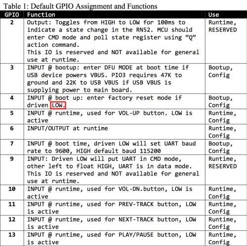
This sent me back to the Microchip site, where I accessed the latest datasheet and command referernce, which in addition to the note above, includes the following description for GPIO4:
Use: Bootup, Runtime, Reserved
Direction: Input
Default: Low
Driving this pin high during bootup will put the module in Factory Reset mode. To reset the module to the factory defaults, this pin should be high on power-up and then toggle low, high, low, high with a 1 second wait between the transitions. During runtime, the module will enter voice command mode if this pin is driven low. Reserved. Not available for reconfiguring as a general purpose IO pin.
This document contradicts the SparkFun table, and adds the runtime behavior.
The presentation is confusing. The pin is listed as "default" low, implying that it either has an internal pulldown, or that an external pulldown should not have any impact. But the description makes clear that driving it high or low will both trigger events, thus indicating that it should be left floating: "During runtime, the module will enter voice command mode if this pin is driven low.".
The evaulation board schematics make clear that it should indeed be left floating, and checking it is something I should have already done.
Unfortunately, if you google "RN52 datasheet", the second result (first PDF) is the old datasheet. Despite being hosted on the Microchip website, this document is out of date.
I promptly removed the pulldown I had attached to GPIO4 and the module came to life, accepting it's configuration and functioning as expected. I've since updated the schematic/board files to use a 3-pin jumper allowing GPIO4 to be driven high/low if required.
2) I almost let the magic smoke out
After solving issue 1, I plugged the daughterboard into the main circuit board and began checking that the MCU could communicate with the external peripherals (RTC, BME280 etc.).
As I was doing this, I noticed the IR LED on the proximity sensor appeared to be glowing#. I grabbed the edges of the board to take a closer look and almost gave myself third-degree burns. I quickly unplugged the board and began to hunt around for the cause.
(#It was not and I don't have IR vision as it turns out. It was the light sensor, which was reflecting a nearby light.)
It was pretty clear that the LED was stuck on, and thus the heat was being generated by the LED, FET, and the 3.6Ω R13 (Update: this was later changed to 1.8Ω to improve the proximity detection range). Per the prior calculations, when on, the resistor is dropping ~1.26V @ 350mA. That's 0.44W. It's a non-branded resistor, but the 1608 (metric) package is typically designed to handle 0.1W.
Of more concern was the LED itself. At ~2V @ 350mA, it was dissipating 0.7W. The datasheet specifies a maximum LED current of 800mA, but that is with a minimum 1/160 duty cycle. I assumed it was toast.
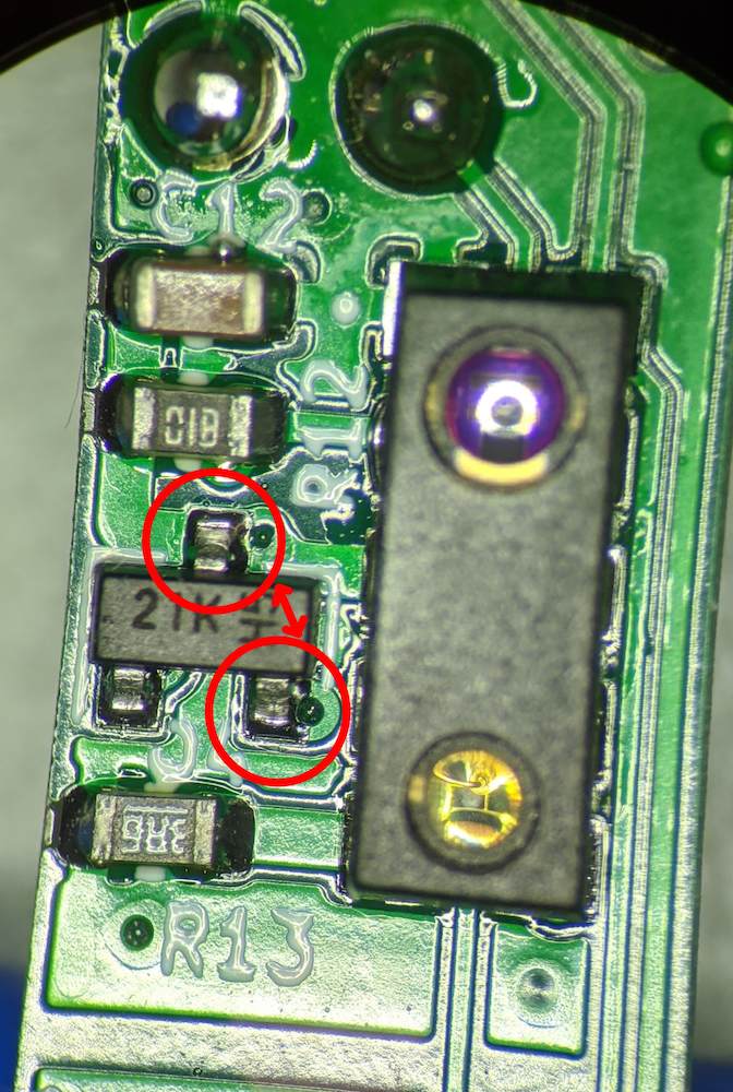
I was pretty sure of the cause once I looked at the schematic. A review of the PCB and FET datasheet solidified it. The FET footprint's drain/source were reversed. KiCad had the correct symbol/footprint match for the part, but I had somehow managed to set the footprint as a generic SOT-23 with the wrong source/drain mapping.
With the source/drain reversed, current flowed directly through the FET's body diode, through the LED and the resistor into ground. The voltage drop across the body diode is likely what saved the LED/resistor, as the actual power dissipation would have been lower than calculated above.
Only 2 of the 3 pins were incorrect, so without using wires, the simplest fix was to flip the package upside down and bend the leads down to the board.
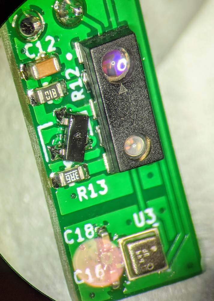
After removing, flipping, and soldering the part back on, I was amazed and relieved to discover that no parts had sustained any damage.
3) 0.3mm FPC sockets are not standardized
I had been successfully using an FPC breakout board during prototyping and had assumed that 0.3mm FPC cables were standardized with respect to the electrode pad spacing and dimensions. They are not.
The PCB design has the FPC socket on the top side and the OLED FPC cable bent 180 degrees. This necessitates an FPC socket with contacts on the top side. I'm using the Panasonic AYF333135.
On inserting the FPC cable into it, it was clear that it didn't fit. The socket is very shallow and the second row of contacts on the cable weren't even partially inside the socket. Reviewing the datasheet showed that the distance from the second row of pads to the tip of the cable should be 0.65-0.75mm. The tip on the OLED cable was >1mm as can be seen below:
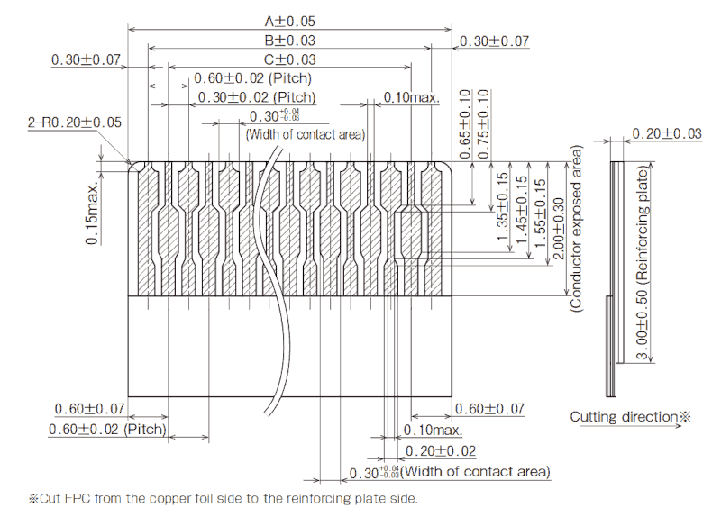
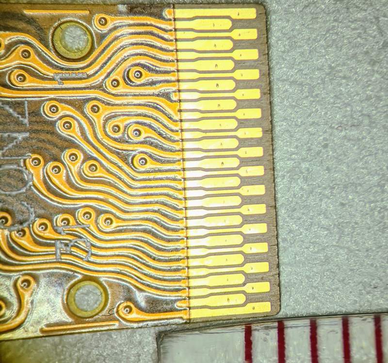
Slicing the end of the FPC cable off with a sharp knife produced the correct dimensions. Since the datasheet includes guidance on cutting, I assume it not atypical to have to do so.
4) I reflowed the board with the OLED capacitors mounted 90 degrees to their correct position :O
In perhaps the most embarrassing issue "encountered", I managed to reflow the OLED capacitors sideways.
This was the result of poor positioning and orientation of the part references on the silkscreen and failing to pay attention to the outlines. I've since reduced the font size on these references and placed them in more appropriate positions.
What would I do differently?
Design and execution issues are inherent in the first revision of any product. Below is a list of the major items I would change if I were to produce a second version:
Use an FPC connector for the daughterboard
Mounting the daughterboard via a pin header meant that perfect alignment was required between the display FPC socket and ALS/proximity sensor, since the display and ALS/proximity sensor cutouts on the facade were fixed. It worked out okay, but it would have been easier to attach the sensors to the facade if the mainboard wasn't hanging off the back of it.
Put the BME280 on a separate PCB
The temperature sensor on the BME280 is not designed to be a standalone sensor. Per the datasheet:
Its output is used for temperature compensation of the pressure and humidity sensors and can also be used for estimation of the ambient temperature...This temperature value depends on the PCB temperature, sensor element self-heating and ambient temperature and is typically above ambient temperature.
The absolute accuracy is (+/-0.5°C @ 25°C and +/-1°C @ 0 -> 60°C).
I separated the ground plane of the sensor from the nearby proximity sensor, but the proximity to the LED resistor and board in general definitely affects the measurements, with readings ~2°C above ambient. I have offset this linearly in software, but the impact is definitely not linear, and a better mounting position (or better still, a dedicated temperature sensor) would give an improved reading.
Use a better haptic motor and shield
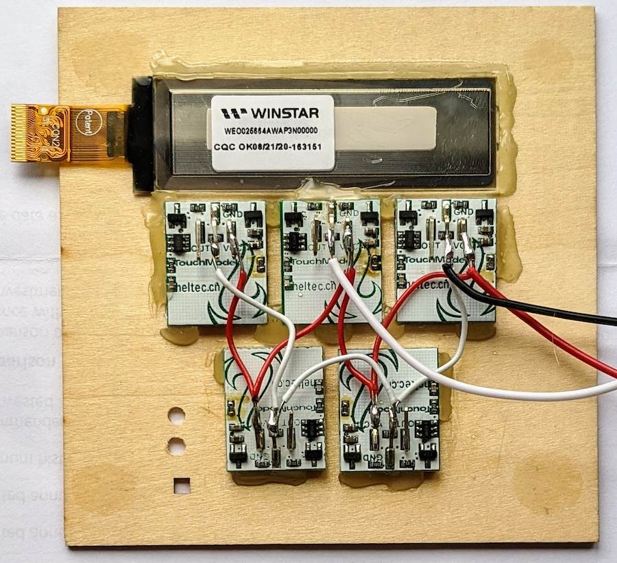
The haptic motor feels quite strong when held in the hand, but once fixed an immovable surface, the vibration produced is meek. The EMR produced by the motor/switching also played havoc with the capacitive buttons, and I ultimately disconnected it.
Put test points on the PCB
The right test points on the PCB would have made life a lot easier during the debugging of the above issues.
Verify the output of the stencil house
I used a new stencil maker for this project. They offer frameless 100x100mm steel stencils for USD2.25 (+USD1.5 shipping), which is hard to beat. I produced the gerber for the paste layer per normal in KiCad, and sent it to them. They sent me back an image of the rendered gerber, which I failed to check properly.
As a result, this is the stencil that I got back:
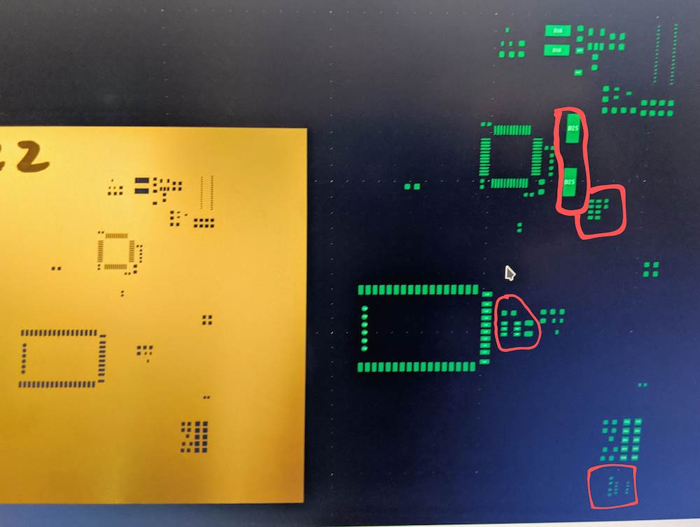
By the time I noticed, I was ready to reflow and so ended up manually applying paste with a toothpick in the missing areas.